


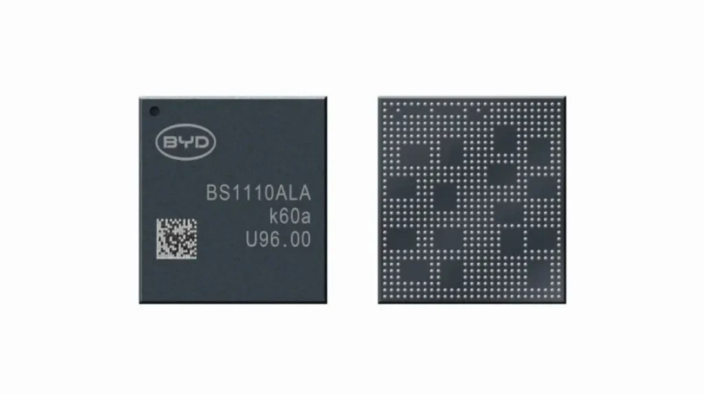
BYD Semiconductor Tuesday that BYD’s chip arm has put a home-grown 4D imaging radar chip into mass production — a part it claims can hold a lock on targets more than 400 meters away and still resolve a parking lock five centimeters off the bumper. The chip is the second half of a vertical stack BYD has been assembling in silence: it follows the May launch of Xuanji A3, China’s first 4nm automotive-grade ADAS processor, which now sits at the center of this radar’s satellite architecture.
Why BYD’s radar needed a fourth dimension
Conventional automotive radar returns three values: range, velocity and horizontal angle. What it does not return is height — and that omission is the reason a radar can see a manhole cover, a low guardrail or a road sign and have no idea whether the object matters. In city traffic, where the difference between a curb and a barrier is the difference between a smooth pass and a hard brake, that blind spot has been the sensor’s defining weakness.
A 4D radar adds elevation. BYD’s part measures range, speed, horizontal angle and vertical angle together, which is what lets it claim the ability to separate a lane from a guardrail, or a car from a pedestrian, at 0.8° of horizontal resolution — and to pick out low, weakly reflective objects such as parking locks, stone bollards and traffic cones at 0.05 m range resolution. That last number is fine enough to feed a 360° parking view and automate pulling in and out of a space. The company frames the coverage as spanning SAE levels L2 through L4: highway navigation, urban driving, automated parking, blind-spot monitoring, adaptive cruise control (ACC), automatic emergency braking (AEB) and lane-change assist, with the radar fusing alongside cameras and lidar to supply redundant perception — the same multi-sensor philosophy that separates Waymo’s 13-camera, 4-lidar stack from camera-only rivals.
BYD’s satellite architecture bet
The more interesting decision is architectural. BYD has built the radar as a satellite: the sensor front end carries no processing of its own, shipping raw data up a MIPI CSI-2 link to the Xuanji A3, which does the compute. The chip pairs that interface with compatibility across mainstream SerDes parts, so it is not hard-wired to BYD’s own silicon — it can be pointed at other ADAS platforms too.
That is a real fork in the road. The traditional “smart sensor” approach gives each radar its own MCU and ships processed object lists over CAN; it is cheap on bandwidth and easy to integrate, but it throws away information before the central computer ever sees it, and it duplicates silicon across every corner of the car. The satellite approach keeps the raw data intact and centralizes intelligence, at the cost of a much heavier data pipe. BYD is betting that pipe is worth it — and that it can afford it because it owns both ends.
The 4D radar chip specs that matter
On the RF side, BYD is claiming first-tier status among production millimeter-wave MMICs. Each of the eight transmit channels puts out 13.5 dBm, with 7-bit phase shifter resolution for beamforming precision. On receive, the noise figure is 11 dB, the input 1 dB compression point is -7 dBm, and the ADC runs at 50 Mbps at 10.5 effective bits — a combination that sets the sensitivity floor and the dynamic range available for picking small targets out of clutter. Phase noise, the spec that governs how well weak returns survive next to strong ones, is quoted at -98 dBc/Hz at 1 MHz offset in the 76–77 GHz band and -96 dBc/Hz in the 77–81 GHz band.
The part is also packaged in a waveguide package, which BYD says improves channel isolation and signal quality while simplifying the RF board layout and cutting system BOM cost. That last point is the one tier-one suppliers will actually price against.
AEC-Q100 Grade 0: qualified for the worst corner
The chip is designed to ISO 26262 ASIL B and qualified to AEC-Q100, with a junction temperature range of -40°C to 150°C. BYD calls that the widest in the industry, and the number is more meaningful than the superlative suggests: 150°C is the ceiling for AEC-Q100 Grade 0, the top temperature grade in the automotive qualification system. Grade 0 is what qualifies a component for under-hood locations. A radar chip that meets it can be mounted almost anywhere on the vehicle, including places where engine-bay heat would rule out a Grade 1 part rated to 125°C. BYD also built in a security algorithm engine for in-vehicle information security.
Why BYD’s 28nm radar chip is not a step backward
The chip is built on 28nm — a process node that looks antique next to the 4nm used for BYD’s own Xuanji A3, and one that invites the obvious criticism. It is the wrong criticism. For millimeter-wave RF, mature nodes are usually the correct engineering answer: analog and RF circuits do not scale the way digital logic does, and the parameters that matter here — noise figure, transmit power, phase noise, matching — are governed by device physics and passive component quality rather than transistor density. Moving to a finFET node would raise cost and mask charges, complicate the RF models, and buy little.
That is why much of the industry’s imaging radar silicon still sits at mature nodes while the ADAS processors beside it race to 3nm. The two chips in BYD’s stack are doing different jobs, and judging the radar by the compute die’s node is a category error. If anything, 28nm is the more defensible choice for a part whose selling price has to survive a tier-one’s BOM review — and it should be friendlier to yield, which matters when the customer is an industry that counts defects in parts per billion.
The Bottom Line
BYD has quietly closed the loop on autonomous-driving silicon: a 4nm compute die in May, a home-grown 8T8R imaging radar feeding it in September, both designed by the same company that builds the car around them. The 400-meter range and 0.05-meter parking resolution are the marketing; the satellite architecture and Grade 0 qualification are the substance. Whether the rest of the industry buys it is still an open question — and it’s the only one that matters.
Sources & Further Reading
- Primary: BYD Semiconductor official announcement (Sept 1, 2026) — 8T8R MMIC, 28nm, satellite architecture, MIPI CSI-2, RF and detection specifications, AEC-Q100 / ISO 26262 ASIL B, -40~150°C junction temperature, product roadmap.
- Corroborating Chinese financial and technology media: Cailianshe (CLS), Securities Times / People’s Financial News, Ifeng Tech, Sina Finance, Mydrivers — consistent on all technical parameters.
- BYD Semiconductor
- BYD — official site
- MIPI Alliance — CSI-2 specification
- SAE J3016 — Taxonomy and Definitions for Driving Automation Systems
- ISO 26262 — Road vehicles, functional safety
- Automotive Electronics Council — official AEC-Q100 documents
- Distributed 4D Millimeter Wave Radar — background explainer
Note on sourcing: this announcement was made in Chinese via BYD Semiconductor’s official channels and reported by Chinese financial media. English-language coverage had not appeared at the time of publication. All technical parameters above were cross-checked across multiple independent Chinese sources and were consistent; interpretation, architectural analysis and the AEC-Q100 Grade 0 context are EVsays’ own.





[…] EVsays — BYD’s 4D radar chip — the sensor side of the same stack. […]